
Table of Contents
Somewhere around the twelfth bitstream revision of the NeoCore bring-up, I found
myself in a familiar corner: the CPU was provably doing something, the screen
was provably showing something, and the two somethings refused to agree. The
oscilloscope could show me any two signals I asked for — but a 65C816 bus
transaction is twenty-six signals wide, and many of the interested signals are within the FPGA.
What I actually wanted was a logic analyzer with a 26-channel pod permanently
soldered to the CPU bus and inside the FPGA.
The "unfair" advantage
Here is the thing about pairing a modern FPGA with a retro-class CPU: the speed
mismatch, which is usually just a fun fact, becomes a debugging superpower.
The NeoCore's W65C816S runs its bus at 3.125 MHz during bring-up. The Lattice
ECP5 fabric around it runs at 50 MHz. That means the FPGA experiences sixteen
clock cycles inside every single CPU bus cycle. From the fabric's point of
view, the CPU is moving in slow motion. Sampling the entire bus — every address
line, every data line, RW — once per CPU cycle costs the FPGA essentially
nothing: one wide register, clocked at a phase of your choosing.
And storing it is nearly free too. One ECP5 block RAM (a single EBR in
pseudo-dual-port mode, 18 kbit) holds 512 complete bus transactions at 25
bits each:
[ RW | A15..A0 | D7..D0 ] --> 25 bits x 512 deep = one EBR
The recorder
The capture side is almost embarrassingly small:
-- once per CPU bus cycle, at a phase where everything is stable
if ph = PH_SAMPLE and not frozen then
    wa    <= std_logic_vector(ptr);          -- pre-increment address!
    word  <= cpu_rw & cpu_a & cpu_d;
    we    <= '1';
    ptr   <= ptr + 1;
end if;
The display you already have
Here is the part I genuinely love. The NeoCore's video output was already
working — and a VGA framebuffer is just a way of showing bits. So the readout
device for the recorder is the machine's own monitor.
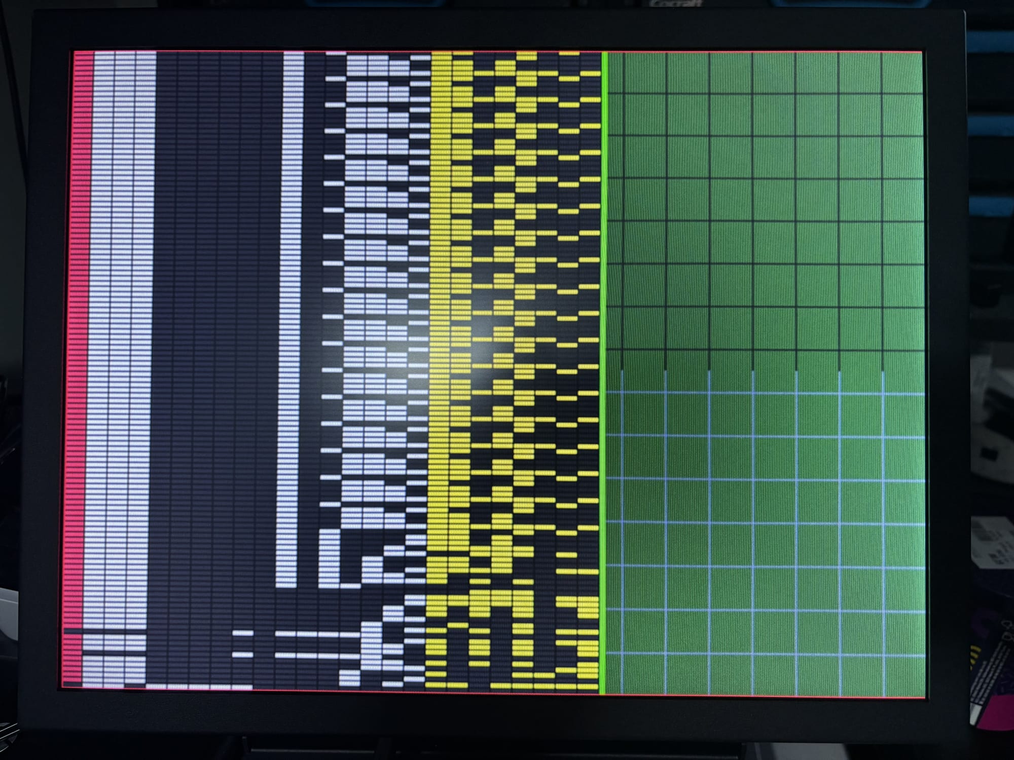
One trace sample per row. Twenty-five fields across, sixteen pixels each:
RW, then A15 down to A0 in white, then D7 down to D0 in yellow. Lit block =
1, dark block = 0. The render logic is a handful of compares off the pixel
counters, plus one block-RAM read per scan-line, prefetched during horizontal
blanking where there are microseconds to spare.
The result is a screen that shows you 120 complete bus transactions at a
glance, oldest at the top, the trigger event at the bottom edge. You can see
program structure as texture: a tight delay loop appears as fine horizontal
striping in the low address bits; the moment the CPU touches the stack, the
high address columns go dark and A8 lights; a three-byte store instruction is
three recognizable rows followed by the write itself.
No host PC, no capture software, no USB dump. The evidence renders at 60 Hz on
the patient's own face.
Did it work?
Yes. Extremely helpful to hunting down bugs in the twilight zone between the 65C816 and the FPGA and all its internal logic.
In fact. So useful that I will include it in the finished product. I will;
- Add a GUI for it.
- Expand it to capture 50 signals both the address bus, but also more internals.
- Add some legends, text, and colors with thought and not just as today randomly.
- Add also some way of displaying certain "variables", i.e. memory locations and what they hold.